Let’s take a quick tour of the Yamaha PSS-A50.
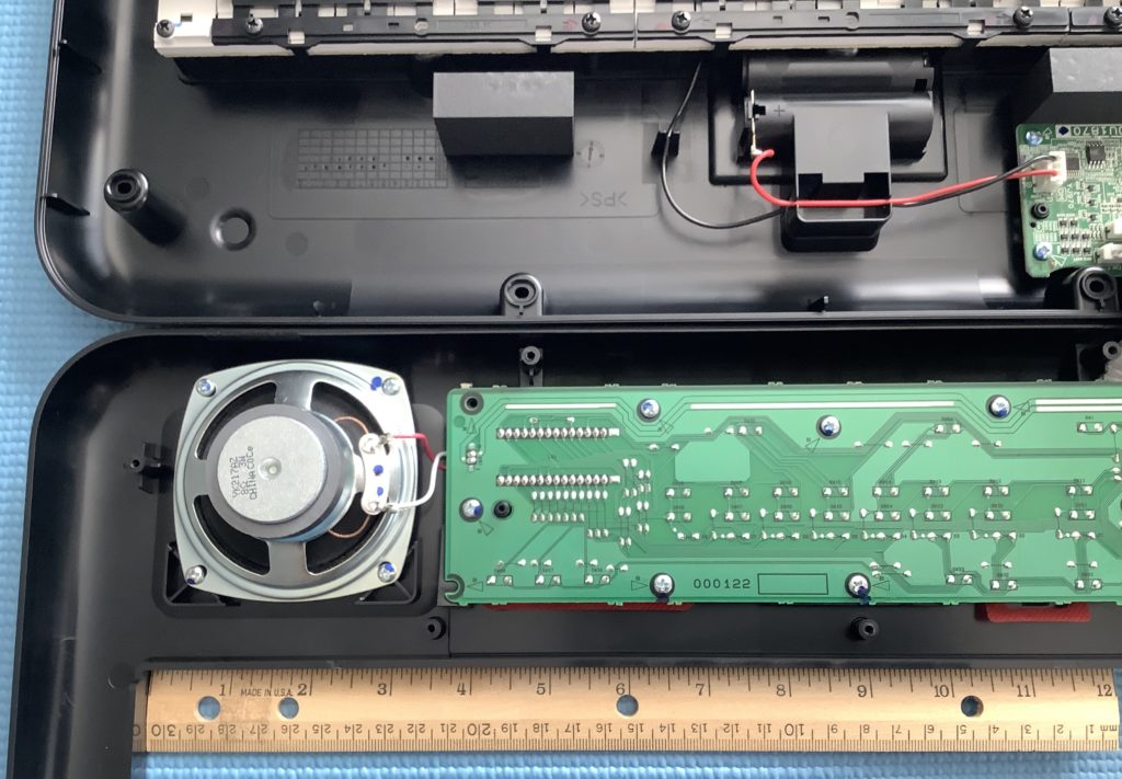
The A50 has two main boards: the digital and analog electronics board (DM) and the front panel board (PN). After removing nine screws — don’t forget the screw hidden in the battery compartment — the A50 splays into two halves: the bottom half containing the battery compartment, DM board and keybed, and the upper half containing the speaker and PN board. The battery connects to a JST XH connector on the DM board. Ribbon cables connect the keybed and the panel board to the DM board.
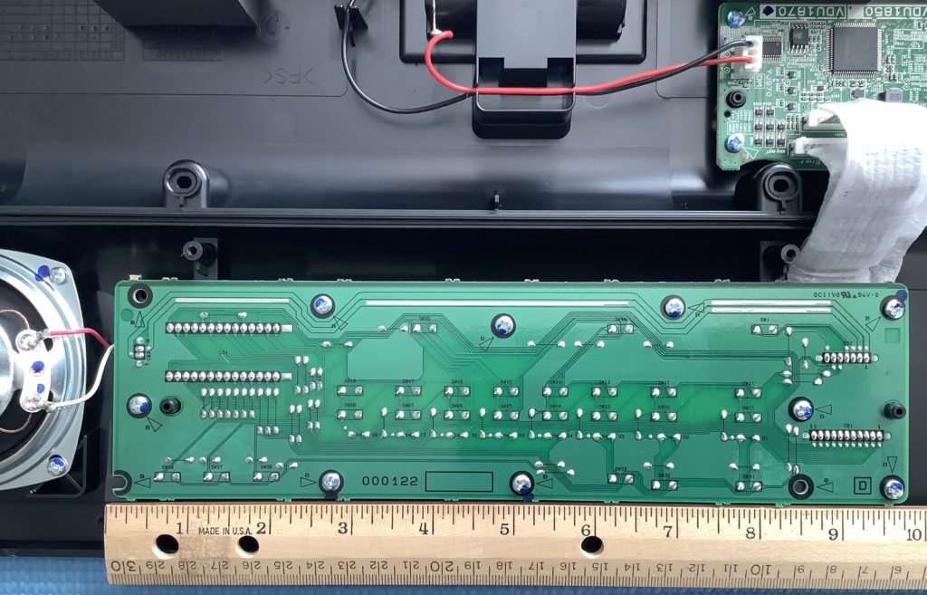
The PN board has traces for the front panel buttons. The buttons are arranged into a 3 by 8 switch matrix: 3 drive lines and 8 sense lines. The power Standby/ON switch has two dedicated lines. The eight sense lines are shared with the three digit LED display. A further 3 lines are devoted to the display (for a total of eight lines). In addition to the front panel switch matrix, the PN board conducts audio signals to the speaker through two wide PCB traces.
I dare to say that the A50, PSS-E30 Remie and PSS-F30 have the same panel board. Only the front panel graphics and software differentiate the models in that regard.
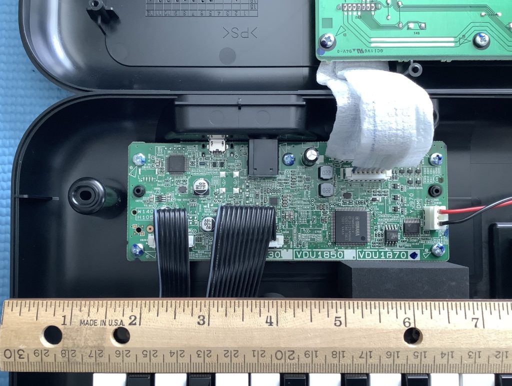
The DM electronics board is tiny and is packed with surface mount (SMT) components. Impressive! The main digital components are:
- Yamaha YMW830-V: Processor and tone generator (IC101)
- Winbond 25Q16JVS1M: 16Mbit Serial flash memory (IC102)
- 74VHC273: 8-bit latch for display data (IC301)
- NXP LPC11U13F/201: USB interface (IC401)
The YMW830-V is also known as “SWLL” and is a Yamaha proprietary system on a chip (SOC). The A50 has separate amplifiers for the speaker (IC701) and headphone output (IC601):
- TI TPA6132A2RTER: Headphone amplifier (IC601)
- Rohm BD27400GUL: Mono class-D power amplifier (IC701)
- NJR NJM2740M: Dual operational amplifier (IC501)
The dual operational amplifier is part of the post-DAC low pass filter. Finally, the power-related components are:
- TI TLV74333PDBVR: 3.3V regulator (IC001)
- TI TPS63060DSCR: Switching regulator (IC004)
- TI TPS25200DRVR: 5V eFuse/power switch (IC006)
The A50 must choose and switch between +5V USB power and battery power. That’s the role of the eFuse/power switch component.
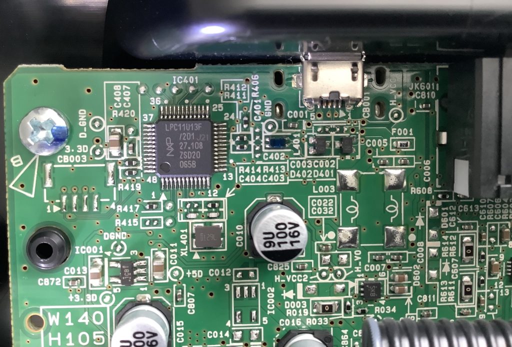
The NXP LPC11U13F is a bit of a surprise to me. It is an ARM Cortex-M0 32-bit microprocessor (MCU) with 24KB of flash memory. The SWLL sends and receives MIDI through its UART RX/TX ports. The ARM LPC converts simple MIDI from the SWLL to MIDI over USB. Using an ARM MCU to do the job seems like over-kill. It goes to show how far we have come as an industry when an MCU can be dedicated to such a mundane task!
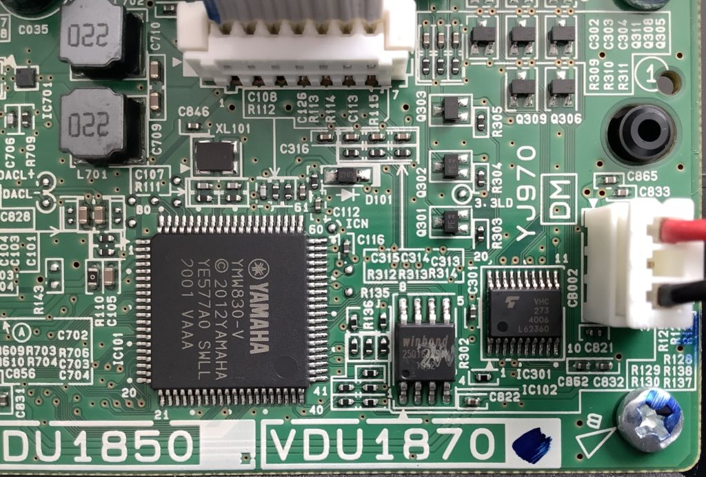
The SWLL (YMW830-V) has many of the specs that we’ve come to know about Yamaha’s entry-level CPUs. The external crystal resonates at 16.9344MHz. The SWLL internal clock is 33.8688MHz and generates a 67.7376MHz master clock. If these numbers look odd to you, simply note that they are even multiples of 44,100Hz, the basic sample rate:
67.7376MHz = 44,100Hz * 1,536
When an external DAC is used, the master clock provides the bit serial audio clock. 1,536 can be subdivided in all sorts of interesting ways depending upon sample word length.
The SWLL integrates host CPU, memory, tone generation, serial MIDI communication, keyboard and front panel scan ports, and display ports. The digital to analog converter (DAC) is also integrated into the SWLL. The SWLL is truly Yamaha’s low-cost system on a chip solution.
The SWLL loads its software and samples from a 16Mbit serial flash ROM. 2MBytes for software and samples is not much, so one wonders if the SWLL has a preprogrammed flash memory of its own?
With the exception of the ARM LPC chip, the A50, PSS-E30 Remie and PSS-F30 electronics are identical. The software and samples determine the product personality. Such a high degree of commonality allows Yamaha to manufacture PSS keyboards (in India) and sell them at a dirt cheap price. Hats off — the amount of technology at this price — less than $100USD — is simply astounding.
Copyright © 2021 Paul J. Drongowski
